|
Prelims : Science & Technology + CA
Mains : GS Paper 3 – Science & Technology; Indigenisation of Technology; Economic Development
|
Why in News ?
India has made a significant advancement in semiconductor research with the development of 3D glass-based semiconductor technology, which is being seen as a potential breakthrough in next-generation chip manufacturing.
- The innovation represents a shift from traditional silicon-based planar chips to multi-layered, high-density chip architectures using glass substrates
- It aligns with India’s broader goal of achieving self-reliance in semiconductor manufacturing and reducing dependence on imports
- The development comes at a time when global semiconductor supply chains are undergoing restructuring due to geopolitical and economic considerations
- It has the potential to position India as a key player in advanced semiconductor packaging and design technologies, even if full-scale fabrication capabilities are still evolving
This breakthrough is significant because semiconductors are the backbone of modern digital economies, powering everything from smartphones to defence systems.
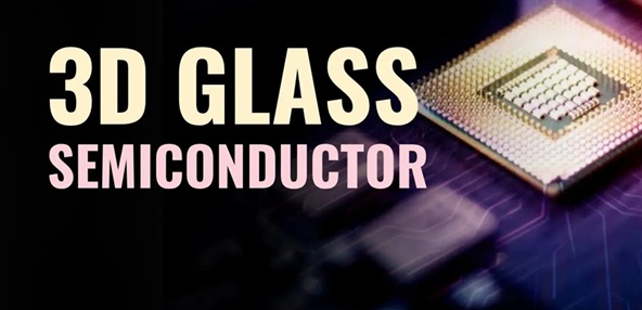
What is 3D Glass Semiconductor Technology ?
3D glass semiconductor technology refers to the use of glass substrates to stack multiple layers of electronic circuits vertically, creating highly compact and efficient chips.
- Unlike traditional chips that are :
- 2D (planar) and spread across a flat silicon surface
- 3D glass technology :
- Enables vertical stacking of components, increasing density and performance
- Glass is used because it offers :
- High thermal stability
- Better electrical insulation
- Lower signal loss
This technology is a part of the broader trend toward advanced packaging and heterogeneous integration, where multiple chip components are combined into a single system.
Key Features of 3D Glass Semiconductor Technology
1. Vertical Integration of Circuits (3D Architecture)
- Multiple layers of circuits are stacked vertically, allowing :
- Higher transistor density
- Reduced footprint of chips
- This leads to :
- More powerful processors in smaller devices
- Efficient use of space in compact electronics
2. Use of Glass Substrates Instead of Traditional Materials
- Glass provides :
- Superior flatness and smoothness
- Excellent thermal resistance
- Reduced electrical interference
- It overcomes limitations of silicon interposers, such as :
- Heat management issues
- Signal distortion
3. Improved Performance and Speed
- Shorter interconnections between layers result in :
- Faster data transmission
- Reduced latency
- This is critical for :
- High-performance computing
- Artificial Intelligence applications
4. Enhanced Energy Efficiency
- Reduced signal loss and efficient heat dissipation lead to :
- Lower power consumption
- Longer battery life in devices
- This is particularly important for :
- Mobile devices
- Data centres
5. Scalability and Future Readiness
- 3D architecture allows :
- Integration of diverse components such as memory, logic, and sensors
- It supports :
- Next-generation technologies like IoT, AI, and 5G
How is it Different from Traditional Semiconductor Technology ?
|
Aspect
|
Traditional (2D Silicon Chips)
|
3D Glass Semiconductor
|
|
Structure
|
Planar (2D)
|
Vertical (3D stacked)
|
|
Material
|
Silicon substrate
|
Glass substrate
|
|
Performance
|
Limited by scaling laws
|
Higher performance due to compact design
|
|
Power Efficiency
|
Moderate
|
High
|
|
Space Utilisation
|
Larger footprint
|
Compact and dense
|
This shift represents a transition from scaling (Moore’s Law) to architecture innovation (3D integration).
Significance for India
1. Boost to Semiconductor Self-Reliance
- India currently depends heavily on imports for semiconductor needs
- Development of advanced technologies like 3D glass chips :
- Reduces dependency
- Strengthens domestic capabilities
- Supports initiatives such as :
- Semiconductor manufacturing missions
- Electronics production
2. Entry into Advanced Packaging Segment
- Semiconductor value chain includes :
- Design
- Fabrication
- Packaging
- India has strong capabilities in :
- 3D glass technology allows India to :
- Enter high-value advanced packaging segment, which is less capital-intensive than fabrication
3. Strategic Importance in Global Supply Chains
- Semiconductors are critical for :
- Defence
- Telecommunications
- Space technology
- Indigenous capabilities enhance :
- Strategic autonomy
- National security
4. Economic Growth and Employment
- Semiconductor ecosystem can :
- Generate high-skilled jobs
- Attract global investment
- It contributes to :
- Manufacturing growth
- Export potential
5. Technological Leapfrogging Opportunity
- Instead of catching up in traditional fabrication, India can :
- Leapfrog into next-generation technologies
- This reduces the gap with :
- Established semiconductor leaders
Challenges in Adoption
1. High Capital and Infrastructure Requirements
- Semiconductor ecosystem requires :
- Significant investment
- Advanced manufacturing facilities
2. Technological Complexity
- 3D integration involves :
- Precision engineering
- Complex fabrication processes
- Requires skilled workforce and R&D capabilities
3. Limited Domestic Ecosystem
- India lacks :
- Fully integrated semiconductor supply chain
- Dependence on imports for :
4. Global Competition
are already leaders in semiconductor technology
5. Policy and Execution Challenges
- Implementation of semiconductor policies requires :
- Efficient coordination
- Long-term commitment
Way Forward
1. Strengthening R&D Ecosystem
- Increase investment in :
- Research institutions
- Industry-academia collaboration
2. Building Semiconductor Infrastructure
- Develop :
- Fabrication units
- Packaging facilities
3. Skill Development
- Train workforce in :
- Chip design
- Advanced manufacturing
4. Global Partnerships
- Collaborate with :
- Leading semiconductor nations
- Technology companies
5. Policy Support and Incentives
- Provide :
- Financial incentives
- Ease of doing business
Practice Questions
Prelims
Q. What is the key advantage of 3D semiconductor technology ?
(a) Increased size of chips
(b) Reduced performance
(c) Vertical stacking for higher efficiency
(d) Elimination of transistors
Mains
“Emerging technologies such as 3D glass semiconductors can help India achieve technological self-reliance.” Discuss.
FAQs
Q1. What is 3D glass semiconductor technology ?
It is a method of stacking circuits vertically using glass substrates.
Q2. Why is glass used ?
For better thermal and electrical properties.
Q3. Why is it important for India ?
It supports self-reliance and technological advancement.
Q4. What is the main challenge ?
High cost and technological complexity.
Q5. What is its future potential ?
Key role in AI, 5G, and advanced electronics.
|


 Contact Us
  New Batch : 9555124124/ 7428085757
  Tech Support : 9555124124/ 7428085757